



Lesson 01
6 min read
From an idea to a file the fab can build.
A chip starts as a specification: what it must compute, how fast, at what power, and with which interfaces. Engineers then describe its behaviour in a hardware description language such as Verilog or VHDL. This is the RTL, register-transfer level. It reads like software, but every line describes hardware that will exist at the same time.
Most of the effort goes into verification, which means proving the RTL does what the specification says before anything is built. Simulation, formal methods and emulation on large FPGA systems all run in parallel. A logic bug found after manufacture costs a new set of masks and months of delay, so teams commonly spend more effort verifying a design than writing it.
Synthesis then turns the RTL into a netlist of standard cells: pre-designed gates and flip-flops supplied for the target process. Place and route positions millions or billions of those cells on the die and draws the wires between them. Timing closure is the long loop of adjusting the layout until every signal arrives within its clock cycle, across every corner of voltage, temperature and manufacturing variation.
- SpecificationWhat and how fast
- RTLVerilog, VHDL
- VerificationSimulate, prove, emulate
- SynthesisRTL to netlist
- Place and routeCells and wires
- Sign-offTiming, DRC, LVS
- Tape-outGDSII or OASIS
The contract with the fab
Everything above is done against the manufacturer's PDK, or process design kit. It contains the design rules, the electrical models of each device, and the technology files the design tools need. Before release, the layout must pass DRC (design rule check: every shape can be manufactured) and LVS (layout versus schematic: what was drawn matches the intended circuit). The final geometry is delivered as a GDSII or OASIS file. Handing it over is still called tape-out, from the days when it went to the fab on magnetic tape.
Lesson 02
6 min read
Masks, lots and the long wait.
The layout is split into layers, and each patterned layer gets its own photomask: a quartz plate carrying that layer's pattern, usually at four times the size it will print. A leading-edge logic chip needs a mask set of many dozens of masks. Writing, inspecting and repairing them is precise and slow, and a full leading-edge set can cost tens of millions of dollars. That cost is paid before a single wafer is made.
Few teams can justify that for a first prototype. A multi-project wafer, or shuttle, puts several customers' designs on one shared mask set and splits the cost between them. Each customer receives a small number of their own dies. A shuttle is how most new designs, test chips and university projects first see silicon.
In the fab, wafers travel in lots of up to 25, carried between tools in a sealed pod called a FOUP. A leading-edge flow runs to more than a thousand individual steps, and many tools visit each wafer again and again. Cycle time, from wafer start to finished wafer, is commonly three to four months at the leading edge. A hot lot is given priority at every tool and can finish much sooner, but every hot lot slows the lots around it, so fabs ration them.
- Wafers per lot
- Up to 25
- Masks in a leading-edge set
- Many dozens
- Process steps
- More than a thousand
- Cycle time
- Typically three to four months
- Mask magnification
- Usually 4×
Lesson 03
7 min read
Yield decides what a chip costs.
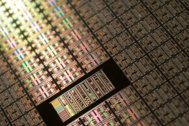
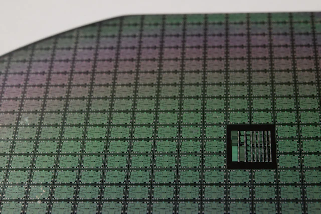
When a wafer is finished, every die on it is tested in place at wafer probe. A probe card lowers fine needles onto each die's pads and runs a short electrical test. The result is a wafer map: a grid showing which dies passed and which failed, and often why. Yield is the share that pass. It is the single number that most affects what a chip costs to make.
Most failures come from defects: a particle, a scratch, a bridge between two wires. The rate at which they land is the defect density, written D₀ and measured in defects per square centimetre. If defects land at random, the simplest model of yield is Y = e−A·D₀, where A is the die area. Real fabs use more refined models, but this one shows the point that matters: yield falls exponentially with area.
- Defect density, D₀
- 0.1 per cm²
- Small die, 1 cm²
- e−0.1 ≈ 90% yield
- Large die, 4 cm²
- e−0.4 ≈ 67% yield
- Near-reticle die, 8 cm²
- e−0.8 ≈ 45% yield
Eight times the area gives half the yield per die, so each good die costs far more than eight times as much. This is the main economic reason large designs are being split into chiplets (lesson 05).
Not every failure is a defect
Defect yield
Dies killed by a random physical fault. Reduced by a cleaner process, and worked around by redundancy, such as spare rows in memory arrays that are switched in at test.
Parametric yield
Dies that work, but too slowly or at too much power. The cause is variation: a film a little thick or a line a little wide. Often it shows as a pattern on the wafer map, such as a weak edge ring.
A sudden drop in yield is an excursion. Finding its cause means tracing the affected wafers back through every tool and chamber they passed, which is why a complete record for each lot matters.
Lesson 04
6 min read
A die is not a product until it is packaged.
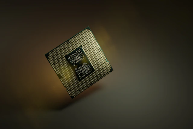
A bare die is fragile, microscopic at its contacts, and impossible to solder to a board. The package protects it, connects its thousands of tiny pads to contacts a board can use, and carries its heat away. Packaging used to be treated as an afterthought. At the leading edge it is now as hard as making the transistors.
A finished 300 mm wafer is about three quarters of a millimetre thick. Backgrinding thins it from the back, often to a few hundred micrometres or much less. Dicing then separates the dies along the streets between them, using a diamond saw, a laser, or stealth dicing, in which a laser weakens a layer inside the silicon and the wafer is split by stretching the tape beneath it.
- BackgrindThin the wafer
- DiceSaw, laser, stealth
- Die attachPlace on substrate
- InterconnectWire or bump
- Underfill, mouldProtect the joints
- Lid, TIMCarry the heat
Wires or bumps
Wire bonding
The die sits face up and fine gold or copper wires loop from pads on its edge to the package. Cheap and proven, and still used for most chips by volume, but connections are limited to the perimeter.
Flip chip
The die is turned face down onto solder bumps spread across its whole surface. That gives far more connections, shorter paths and better power delivery. Processors and accelerators all use it.
Beneath a flip-chip die sits the substrate, a small multilayer circuit board that fans the bumps out to a ball grid the main board can take. Underfill fills the gap under the die so the joints survive the die and substrate expanding at different rates as they heat. On high-power parts a metal lid spreads heat, coupled to the die by a thermal interface material.
Lesson 05
7 min read
Building one system from many dies.
Two limits push large designs apart. The reticle caps a single die at roughly 850 mm², and lesson 03 showed that yield falls steeply as dies grow. The answer is chiplets: several smaller dies, each made and tested separately, joined in one package so tightly that they behave almost like one chip. Each chiplet can also use a different process. Compute might sit on the newest node while I/O stays on an older, cheaper one.
The dies have to talk to each other over very short, very dense links. Advanced packaging is the set of ways to build those links.
| Approach | How the dies connect | Typical pitch | Used for |
|---|---|---|---|
| 2.5D silicon interposer | Side by side on a large slab of silicon carrying fine wiring | Micro-bumps, tens of µm | AI accelerators with HBM |
| Silicon bridge | Small silicon pieces embedded only under the die edges | Micro-bumps, tens of µm | Dense links without a full interposer |
| Fan-out | Dies set in mould compound with wiring built on top | Coarser, a few µm lines | Mobile processors, cost-sensitive chiplets |
| 3D, micro-bump | Stacked face to back through TSVs and small solder bumps | Roughly 20 to 50 µm | HBM memory stacks |
| 3D, hybrid bonding | Copper pads fused directly, no solder | Under 10 µm, falling | Stacked cache, image sensors |
Through-silicon vias and HBM
A through-silicon via (TSV) is a copper-filled hole that runs vertically through a thinned die, so signals and power can pass straight up into the die above. High-bandwidth memory (HBM) is built this way: a stack of 8, 12 or 16 DRAM dies on a base die, joined by thousands of TSVs and presenting an interface over a thousand bits wide. Placed beside the processor on an interposer, a few HBM stacks deliver terabytes per second. That bandwidth is the main reason the memory wall from course 01 has not stopped AI hardware.
For chiplets from different sources to work together, the links between them need a common standard. UCIe (Universal Chiplet Interconnect Express), launched in 2022, is an open specification for die-to-die links that is now widely adopted.
Lesson 06
6 min read
Test, and test again.
A chip with billions of transistors cannot be tested by trying every input. Test is designed in from the start. Scan chains link the chip's flip-flops into long shift registers, so a tester can load any internal state, run one clock and read the result back. Software generates the patterns that exercise as many possible faults as it can. Built-in self-test (BIST) circuits let memories and other blocks test themselves at full speed.
The patterns run on automatic test equipment (ATE): large, expensive machines that drive and measure thousands of pins at once. Test time costs money, so test engineers trade coverage against seconds per part.
- Wafer probeEvery die, in place
- Known-good dieFuller test before stacking
- Final testThe packaged part
- Burn-inHeat and voltage stress
- System-level testReal software, real board
- BinningSort by speed and power
A known-good die has been tested thoroughly enough before packaging to be trusted inside an expensive multi-die stack. Burn-in runs parts hot and at raised voltage for a period, so weak parts that would fail early in service fail on the test floor instead. System-level test boots the part on a real board and runs real workloads, which catches faults structural tests miss.
Binning
Dies from the same wafer are not identical. Test sorts them into bins by the clock speed they reach and the power they draw, and those bins become different products at different prices. A die with one faulty core can often be sold with that core switched off. Binning is why one design can appear as a whole product line.
Lesson 07
6 min read
Who makes what.
Until the late 1980s, most chip companies designed and made their own parts. Rising fab costs split the industry into specialists. Today almost every chip passes through several companies on its way to a board.
| Role | What it does | Owns a fab |
|---|---|---|
| IDM | Integrated device manufacturer: designs and makes its own chips | Yes |
| Foundry | Manufactures chips designed by others | Yes |
| Fabless | Designs chips and has a foundry make them | No |
| OSAT | Outsourced assembly and test: packages and tests other companies' dies | Packaging and test lines |
| EDA and IP | Sells the design software, and licensed blocks such as processor cores and interfaces | No |
| Equipment and materials | Builds the tools, and supplies wafers, gases, chemicals, photoresists and masks | No |
The cost of the leading edge
A leading-edge logic fab now costs on the order of twenty billion dollars or more, and a single EUV lithography scanner costs well over a hundred million. Few companies can carry that, so the number making leading-edge logic has fallen to a handful. Each layer of the supply chain is concentrated in the same way. EUV scanners come from a single supplier. Design software is dominated by a few firms. Most leading-edge logic is made in Taiwan, and memory production is concentrated in South Korea. Much of the world's assembly and test happens across Taiwan, China and Southeast Asia.
That concentration is why governments in the United States, Europe, Japan and elsewhere are now subsidising new fabs, and why where a chip is made has become a question of policy as well as cost.
- Leading-edge fab
- On the order of $20 billion or more
- EUV scanner
- Well over $100 million each
- Leading-edge mask set
- Up to tens of millions of dollars
- Companies at the leading edge
- A handful
Knowledge check
8 questions
Check yourself.
Next course