

Lesson 01
6 min read
From sand to a perfect crystal.
Every chip starts as quartz, which is silicon dioxide. Heated with carbon in an electric arc furnace, quartz gives up its oxygen and leaves metallurgical-grade silicon, about 98 to 99 percent pure. That is good enough for aluminium alloys and solar-grade refining, and nowhere near good enough for a transistor.
To go further, the silicon is turned into a gas, purified, and turned back into a solid. In the Siemens process it reacts with hydrogen chloride to form trichlorosilane, a liquid that can be distilled until almost nothing else remains. The vapour is then decomposed onto heated rods, which grow into thick bars of polysilicon at nine to eleven nines of purity.
Polysilicon is made of many small crystals; a transistor needs one. In the Czochralski method, polysilicon is melted in a quartz crucible just above 1,414 °C, a small seed crystal is dipped into the melt, and the seed is drawn slowly upward while turning. The silicon freezes onto it in the same orientation, atom by atom, forming a single-crystal boule that can be around two metres long and weigh several hundred kilograms. Dopant added to the melt sets the wafer's starting type.
- QuartzSilicon dioxide
- Metallurgical SiAbout 99% pure
- Polysilicon9 to 11 nines
- BouleOne crystal
- SliceWire saw
- Polished waferReady for the line
Slicing and finishing
The boule is ground to an exact diameter, marked with a small notch that records its crystal orientation, and cut into wafers with a wire saw. A 300 mm wafer is about 0.775 mm thick. Grinding, etching and chemical-mechanical polishing then leave one face flat and smooth to within a few atoms across its whole surface. For many processes a thin epitaxial layer of especially clean crystal is grown on top before patterning begins. 300 mm has been the leading-edge standard since the early 2000s; a move to 450 mm was studied and abandoned.
Lesson 02
5 min read
The cleanest rooms there are.
A modern transistor's features are a few tens of nanometres across. A particle a fraction of that size, landing at the wrong step, can short two wires or block a pattern and kill a die. Ordinary city air carries tens of millions of particles half a micrometre or larger in every cubic metre. A fab removes nearly all of them.
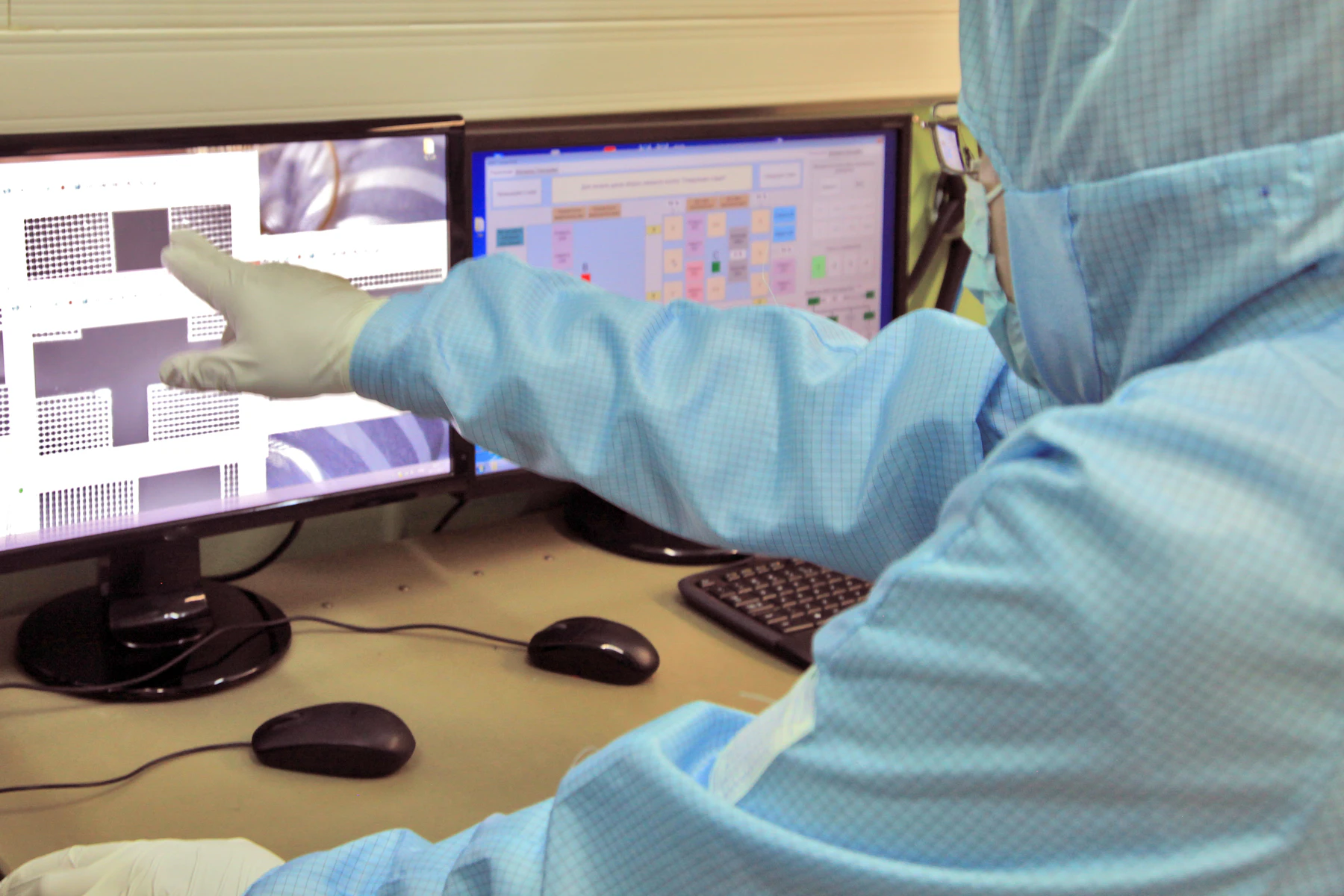
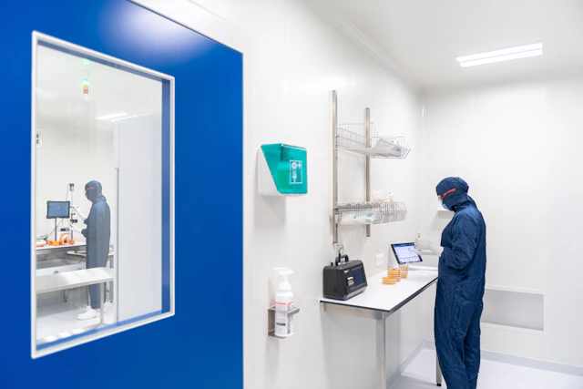
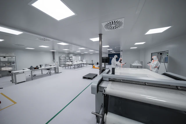
Cleanliness is graded under ISO 14644-1 by the number of particles allowed per cubic metre. Filtered air is pushed down from the ceiling and out through the floor in a steady flow, so anything shed is carried away rather than settling. People are the largest source of contamination, which is why staff wear full gowns, hoods, masks and gloves.
| Class | Max particles ≥ 0.5 µm per m³ | Typical use |
|---|---|---|
| ISO 3 (Class 1) | 35 | Inside tools and wafer enclosures |
| ISO 5 (Class 100) | 3,520 | Process bays |
| ISO 7 (Class 10,000) | 352,000 | Assembly and test halls |
| Outdoor city air | Tens of millions | For comparison |
The wafer rarely sees the room
In a modern fab the cleanest air is not the room's but the box's. Wafers travel in sealed pods called FOUPs, each holding 25, carried on overhead rails between tools. A pod docks to a tool and opens into a small enclosure that is cleaner than the bay. People supervise, but the wafers are moved by machines.
Ultrapure water
Wafers are rinsed many times along the flow. The water is purified to around 18.2 MΩ·cm, the theoretical limit for pure water, and a large fab uses millions of litres a day.
Chemicals and gases
Hundreds of high-purity gases, acids, solvents and precursors feed the tools, delivered through sealed lines and monitored for contamination at parts per billion or lower.
Lesson 03
8 min read
Printing with light.
Lithography decides where every other step acts. The wafer is coated with photoresist, a light-sensitive polymer. A scanner shines light through a mask (or reticle) holding one layer of the design, and its lenses shrink the image, usually four times, onto the wafer. Where light lands, the resist's chemistry changes, and a developer washes either the exposed or unexposed parts away. What remains is a stencil for the next etch or implant.
- CoatSpin on resist
- BakeSet the film
- ExposeScanner, through the mask
- DevelopReveal the pattern
- EtchTransfer it down
- StripRemove the resist
A chip is built by repeating that loop for each patterned layer, often dozens of times. The scanner steps across the wafer, exposing one field at a time, each lined up to the layers already there.
The resolution equation
The smallest feature a scanner can print is proportional to the wavelength of its light divided by the numerical aperture (NA) of its optics, times a process factor called k₁. Every advance in lithography has cut the wavelength, raised the NA or squeezed k₁.
| Generation | Wavelength | NA | Notes |
|---|---|---|---|
| KrF DUV | 248 nm | Up to about 0.9 | Still used for less critical layers |
| ArF DUV, dry | 193 nm | Up to about 0.93 | Workhorse for many layers |
| ArF immersion | 193 nm | 1.35 | Water between lens and wafer raises the NA above 1 |
| EUV | 13.5 nm | 0.33 | Critical layers at the leading edge |
| High-NA EUV | 13.5 nm | 0.55 | Entering use; half the exposure field |
Multi-patterning and EUV
When 193 nm immersion reached its limit, fabs printed one layer in several passes. Multi-patterning splits a dense pattern over two or more exposures, or uses spacer films grown on a printed line to double or quadruple its density. It works, but every extra pass adds cost, time and another chance for misalignment.
EUV lithography, at 13.5 nm, prints many of those layers in one pass. Producing the light means hitting tiny droplets of molten tin with a high-power laser to make a plasma. Almost every material absorbs EUV, including air and glass, so the whole path runs in vacuum and uses mirrors coated with alternating molybdenum and silicon layers instead of lenses. The mask is reflective too. ASML is the only supplier of EUV scanners.
Printing the right shape is only half the job. Each layer must also land on the one beneath it. That alignment, called overlay, is held to a few nanometres at the leading edge.
Lesson 04
7 min read
Adding and removing material.
Lithography decides where. Deposition and etch do the building. Most of the steps in a fab add a thin film to the whole wafer, then remove it everywhere the resist does not protect.
Putting films down
| Method | How it works | Used for |
|---|---|---|
| Thermal oxidation | Silicon reacts with oxygen or steam at high temperature | High-quality silicon dioxide grown from the wafer itself |
| CVD | Gases react on or near the hot surface and leave a solid film | Insulators, polysilicon, tungsten |
| PVD (sputtering) | Ions knock atoms off a solid target onto the wafer | Metal barriers, liners and seed layers |
| ALD | Two gases take turns; each reaction stops by itself after one atomic layer | Gate insulators, conformal coatings in deep or narrow features |
| Epitaxy | Crystal grown so it continues the wafer's own lattice | Channel layers, silicon-germanium, source and drain |
Atomic layer deposition deserves a second look. Because each cycle is self-limiting, the film grows by a fixed fraction of a nanometre per cycle, evenly over every surface, including the sides of trenches and under the sheets of a gate-all-around transistor. It is slow, so it is used where precision matters more than speed.
Taking films away
Wet etching dissolves material in a liquid. It is clean and selective, but it eats sideways as fast as downward, which is useless for features narrower than the film is deep. Plasma (dry) etching uses reactive ions driven straight down by an electric field, so it cuts vertical walls. That directionality is called anisotropy.
Selectivity
How much faster an etch removes the target film than the mask above it or the layer below. High selectivity lets the etch stop cleanly where it should.
Aspect ratio
Depth divided by width. Memory chips need holes fifty or more times deeper than they are wide, and keeping them straight to the bottom is among the hardest problems in the fab.
Atomic layer etch
The mirror of ALD: alternate steps modify and then remove one surface layer at a time. Used where a few atoms too many would change how the device behaves.
Clean
Between steps, wafers are cleaned of residue, particles and stray metal. Cleans are among the most frequent steps in the whole flow.
Lesson 05
5 min read
Doping, and the heat that fixes it.
Course 01 explained that transistors are made of n-type and p-type regions. In the fab, most of those regions are made by ion implantation. Dopant atoms such as boron, phosphorus or arsenic are ionised, sorted by mass in a magnetic field, accelerated, and fired into the wafer. Resist or hard masks block them wherever they are not wanted.
Two settings control the result. Energy, from a few hundred electron-volts to millions, sets how deep the ions go. Dose, the number of ions per square centimetre, sets how many arrive. Together they set the doping profile.
Implantation is violent. Each ion knocks silicon atoms out of place, and most dopants come to rest between lattice sites where they do nothing electrically. An anneal heats the wafer to repair the crystal and pull the dopants into lattice sites, which is called activation.
The thermal budget
Heat also makes dopants spread out, and a junction that spreads a few nanometres can ruin a modern transistor. So annealing has become shorter and hotter. A furnace anneal takes tens of minutes, a rapid thermal anneal takes seconds, and flash and laser anneals heat only the top of the wafer for a millisecond or less. Each wafer has a thermal budget (total heat over time), and every later step has to fit inside what is left of it. That is one reason metal wiring, which cannot take much heat, is built last.
At the leading edge, some regions are doped as they are grown instead: the source and drain of a FinFET or nanosheet transistor are usually epitaxial crystal with the dopant added in the gas.
- Implant energy
- Sub-keV to MeV
- Implant dose
- About 10¹¹ to 10¹⁶ ions per cm²
- Rapid thermal anneal
- Seconds
- Flash or laser anneal
- Milliseconds or less
Lesson 06
7 min read
Wiring billions of switches together.
The flow divides into three parts. The front end of line (FEOL) builds the transistors in the silicon. The middle of line (MOL) makes the tiny contacts that reach down to each source, drain and gate, often in tungsten or cobalt. The back end of line (BEOL) builds the wiring: a stack of copper layers separated by insulator and joined by vertical vias.
A leading-edge logic chip has roughly 10 to 20 metal layers. The lowest are the narrowest and connect neighbouring transistors. Each layer up is wider and spaced further apart, ending in thick top layers that carry power and long-distance signals across the die.
Damascene: wires made by filling, not cutting
Copper conducts better than aluminium, which it replaced in the late 1990s, but it does not plasma-etch cleanly. So fabs reversed the process. Instead of patterning a metal film, they etch trenches in the insulator and fill them with metal, an approach named after the inlaid metalwork of Damascus. In dual damascene the via and the trench above it are filled in one go.
- DepositLow-k insulator
- PatternVias and trenches
- LineBarrier and seed
- PlateCopper fill
- PolishCMP back to flat
- CapSeal the copper
Chemical-mechanical polishing (CMP) grinds the wafer flat with a pad and a chemical slurry, removing the excess copper and leaving metal only in the trenches. Without it, every layer would add to the bumps of the ones below, and the next exposure could not be focused.
The insulator between wires matters as much as the wires do. Two lines side by side form a capacitor, and charging it costs time and energy. Low-k dielectrics, often carbon-doped and porous oxides, reduce that capacitance, at the cost of being mechanically fragile. And, as course 01 noted, the newest processes move power wiring to the back of the wafer entirely, leaving the front stack for signals.
Lesson 07
6 min read
You can only make what you can measure.
A leading-edge flow runs to well over a thousand steps, and an error at step 200 may not show up as a failure until the wafer is tested months later. So the line measures as it goes. Metrology checks that each step did what it should. Inspection looks for what should not be there.
CD-SEM
A scanning electron microscope measures critical dimensions, the width of lines and spaces, directly from the image.
Scatterometry
Light reflected from a repeating test pattern is matched to a model, recovering shape, depth and sidewall angle quickly and without damage.
Overlay and film
Dedicated targets show how far one layer sits from the last. Ellipsometry and similar optical methods measure film thickness.
Defect inspection
Optical tools scan whole wafers for particles and pattern faults. Electron-beam tools review and classify what they find, and catch faults too small for light.
Closing the loop
Statistical process control plots each measurement against its limits and flags a tool that is drifting before it produces scrap. Advanced process control goes further. Run-to-run control feeds each lot's results back into the recipe for the next lot, and feed-forward passes one step's measurement on so the next step can compensate. For example, an etch can be adjusted for a line that printed slightly wide.
| Quantity | Typical value |
|---|---|
| Wafer diameter | 300 mm |
| Wafers per lot | Up to 25, one FOUP |
| Process steps | Over 1,000 |
| Mask layers | Several dozen |
| Metal layers | About 10 to 20 |
| Cycle time, start to finished wafer | About three to four months |
| Overlay tolerance | A few nanometres |
Knowledge check
8 questions
Check yourself.
Next course